
PRODUCTS
- 首頁
- 經營品牌
- Advanced Spectral Technology(AST)
- 精密量測系統
- AST-Zentura
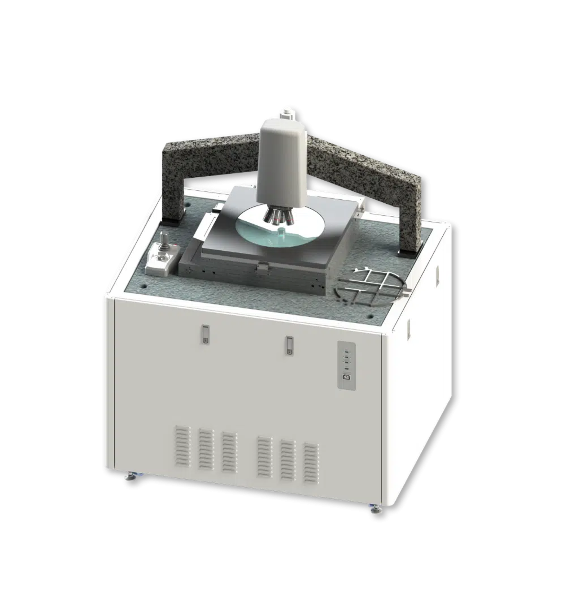
AST-Zentura
Zentura Wafer-Level Metrology System
Wafer level metrology solution provides flexible sensor integration options
。AS4000 – Optical Stylus
.Wafer Shape – Bow, Warp, Flatness, etc.
. Step Height / Depth Measurements
. Multiple Measurement Range / Resolution options
。 AS5000 – White Light Thickness Metrology
. Ultra-thin Silicon (1 to 50µm) Thickness Mapping
. Thickness Mapping of Photoresist, Adhesive Layer
。 AS6000 – IR Thickness Metrology
. Silicon (10 to 1200u)Thickness mapping
. Adhesive Thickness After Bonding
. Etch Depth Measurement
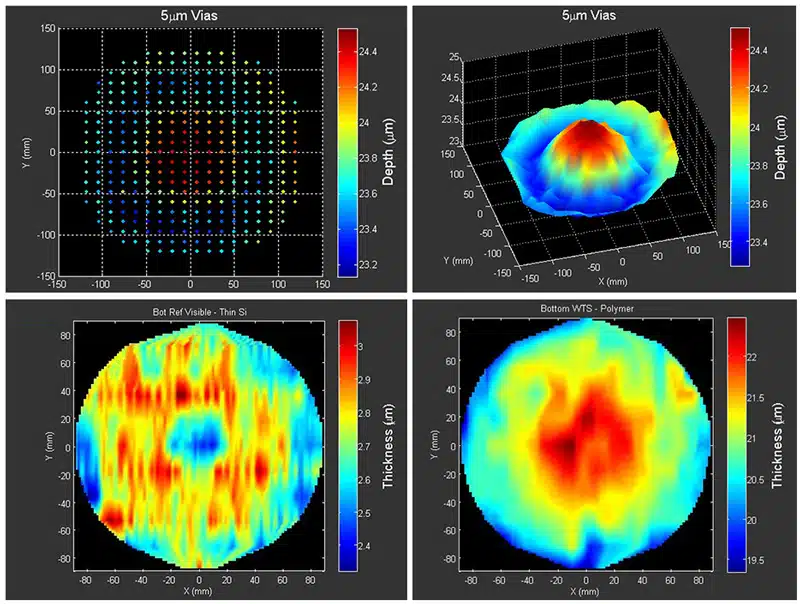
AST-Zentura supports a range of measurement technologies integrating advanced flexible sensor options developed to address critical wafer processing applications within an automated turnkey system solution. Configuration options include wafer sizes from 50mm to 300mm, with & without wafer handling.
。Precise wafer thickness including multi-layer measurement from 10-1200 microns
。Bonded wafer adhesive layer & photoresist layer measurement from 1 to 50 microns
。Etch depth measurements: Trenches down to 1um width / Via down to 1um diameter
。Capability to perform vision-based measurements validating line-width, feature diameter, alignment, and more with accuracy of < 0.1µm
。High Throughput, up to 60 WPH
。Wafer Shape: Bow, Warp, Flatness
。Thickness Mapping: TTV, Avg, STD, TIR, Min/Max
。Thickness mapping of photoresist, adhesive
。Adhesive thickness measurement after bonding
。REtch Depth Measurement: TSVs, TGVs, Trench, etc.
Platform
‧300mm x 300mm X-Y Travel
‧100mm Z-axis Travel
‧ISO 5 (Class 100) Cleanroom Compatible
‧ISO 4 (Class 10) Cleanroom Option
‧Semi S2 / S8 Protocol Compliant
Optics
‧Microscope with High-Resolution camera
‧5X, 10X, 20X, 50X Objectives
‧Brightfield LED Light Source
Software
‧ScopeViewer3 Software Application Suite
‧Flexible Part-Programming
‧Advanced Vision Tools & Metrology Features
‧SECS-GEM factory Interface
‧Full Recipe Control of all Imaging Functions
‧Recipe Generation in Python Layer
Wafer Handling Option
‧System can be configured with or without wafer loader
‧Standard: Supports 50mm to 200mm wafers Open Cassette
‧Optional: SMIF, FOUP, 300mm Wafers, Film Frame, etc.