
冲成股份有限公司
AST-WDI

AST-WDI

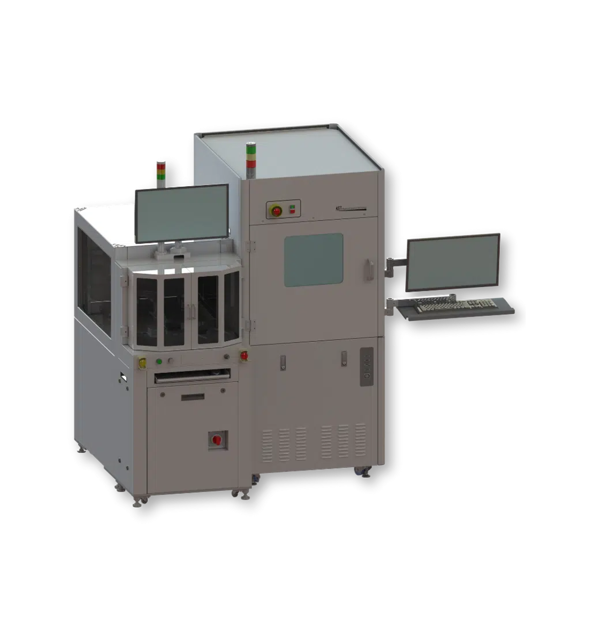
Wafer & Die Inspection System
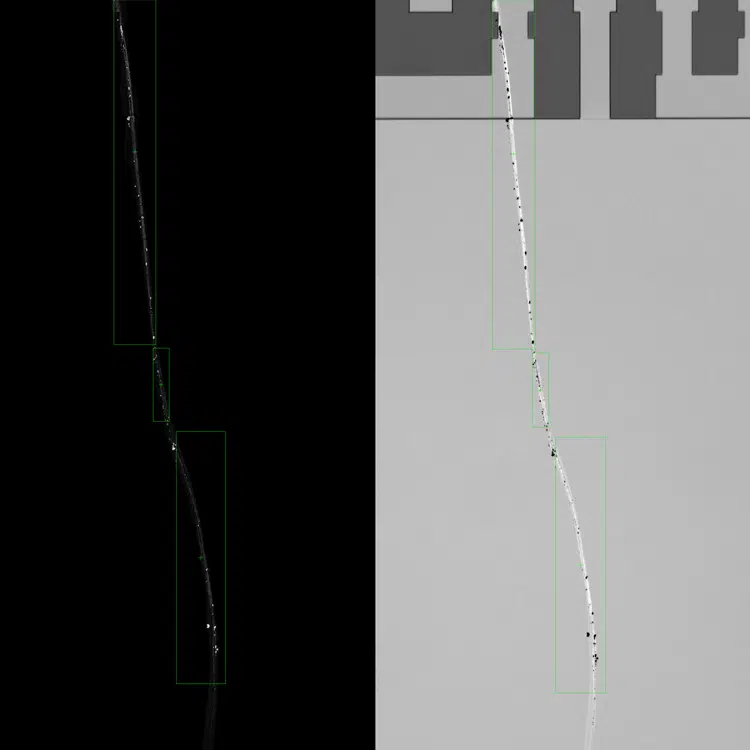
The AST-WDI defect detection system delivers high-precision quality assurance for semiconductor manufacturing, identifying microscopic defects with sub-micron accuracy. This advanced inspection platform integrates seamlessly into production environments, detecting particles, scratches, and pattern irregularities early in the manufacturing process to maintain optimal yields and process control.

The AST-WDI platform combines sophisticated AI capabilities with multi-spectral imaging technology to perform comprehensive wafer and die-level quality assessments. The system features a flexible configuration with high-resolution optics and multiple illumination options to detect even the most challenging defects across various semiconductor applications.


300mm x 300mm X-Y travel with 100mm Z-axis capability

Configurable with multiple wafer handling options: open cassette (50mm-200mm), SMIF (200mm), and FOUP (300mm)

High-resolution optical system supporting 5X to 100X brightfield and darkfield objectives

ACompatible with ISO 5 cleanroom environments, with ISO 4 option

Comprehensive dimensional measurement tools including video edge detection and geometric constructions

Advanced ScopeViewer3 Software with AI-powered defect detection algorithms

Advanced Thickness Measurement Technology – Precisely measure Through Silicon Vias (TSVs), Wafer/Layer Thickness, Photoresist thickness, etc.


Detection of sub-micron defects including particles, scratches, and pattern irregularities

Pattern verification to confirm accurate replication of complex semiconductor designs

Quality assurance and process control monitoring for manufacturing yield optimization

Wafer-level inspection for early defect identification

Die-level inspection for final quality verification

Custom inspection solutions for specialized semiconductor components

TSV depth Measurements

Film / Photoresist Thickness Measurements
Illuminiation

‧Brightfield, Darkfield, Kohler Illumination

‧Optional Infrared (NIR & SWIR) Illumination with5-Position Filter Wheel


Optics

‧High-Resolution Optical System supporting

‧5X, 10X, 20X, 50X, & 100X BF & DF objectives

‧Standard Video Auto-Focus

‧Optional Tracking Laser Auto-Focus

Software

‧ScopeViewer3 Software Application Suite

‧Flexible Part-Programming

‧Advanced Vision Tools & Metrology Features 

‧SECS-GEM factory Interface 

‧Full Recipe Control of all Imaging Functions

‧Recipe Generation in Python Layer

‧Flexible Configuration for Long Term Support of Hardware and Software Components


Wafer Handling Option

 ‧System can be configured with or without wafer loader

 ‧Open cassette – wafers & film frames (50mm to200mm)

 ‧SMIF (200mm wafers) & FOUP (300mm wafers)

 ‧Custom die-level carrier & packaging assembles