
冲成股份有限公司
AST-CDO

AST-CDO

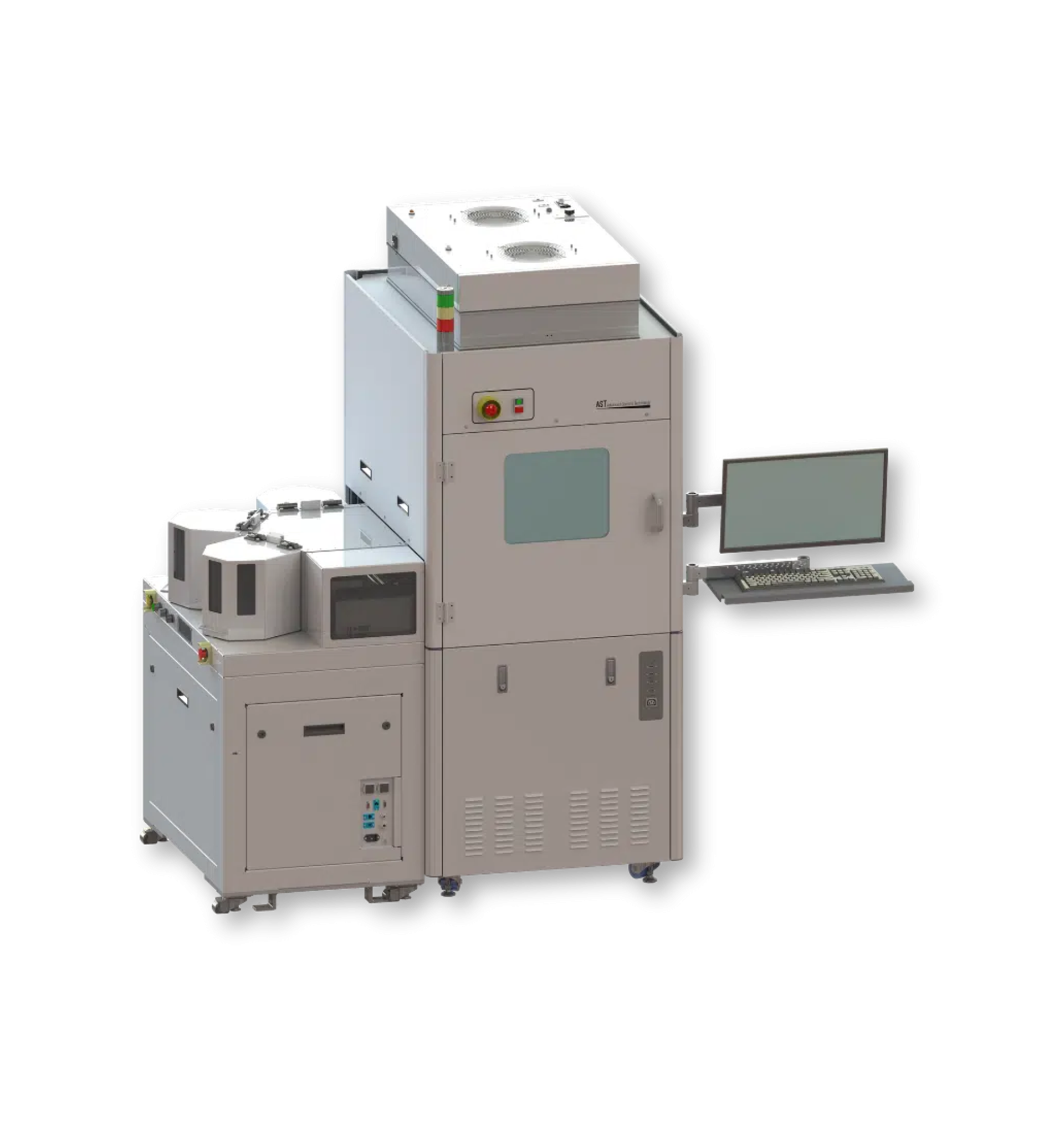
CD & Overlay Metrology System

The AST-CDO metrology system provides a high-precision measurement solution for validating critical dimensions and ensuring accurate alignment verification between layers on bonded and multi-layer semiconductor wafers. This advanced metrology system provides superior optical-based measurement technology with automated wafer handling configurations for achieving optimum performance and capability.

AST's CD & Overlay Metrology System utilizing advanced measurement technology to ensure critical wafer features are within tolerance to achieve optimum performance and ensure wafer processes and specifications remain in control.  The capability to image through layers of the wafer to detect any misalignment caused by mask errors, process variations, and equipment inaccuracies during manufacturing are identified with a high-degree of precision and performance.  The ability of the AST-CDO system to be configured and implement tunable wavelength specific imaging of an overlay alignment pattern through multiple-layers of a wafer that may consist of differences of the material properties and characteristics that impact image quality and contrast for confirming layer-to-layer overlay alignment.  The AST-CDO system addresses and optimizes the measurement performance of each layer based on its wavelength transmission properties.


Multi-spectrum imaging configurations including visible, NIR, SWIR, & UV

Fully automated operation with recipe-driven measurement capability

Fully integrated EFEM wafer handling automation solutions supporting 50mm to 200mm wafter cassettes with 1, 2, or 3 load-ports

SECS GEM network integration for factory automation compatibility

CD measurement repeatability down to 5nm capability

Overlay metrology repeatability down to 10nm capability

300mm wafer handling options available, including support FOUP (300mm) and SMIF (200mm) load ports

Comprehensive data analysis and reporting tools


Overlay verification for multi-layer device fabrication and wafer-to-wafer bonding

Compound Semiconductors

3D stacking of chips and dies (chip on wafer alignment verification)

Power devices, MEMS device critical dimension and overlay inspection

Flip Chip / Hybridization alignment verification

Photonics devices critical dimensional verification

。Advanced packaging alignment verification

。Process control solution to monitor & adjust alignment of lithographic layers during manufacturing process
Platform

‧300mm x 300mm X-Y Travel

‧100mm Z-axis Travel

‧ISO 5 (Class 100) Cleanroom Compatible

‧ISO 4 (Class 10) Cleanroom Option

‧Semi S2 / S8 Protocol Compliant


Optics

‧High-Resolution Optical System supporting

‧5X, 10X, 20X, 50X, & 100X Objectives

‧Optional 150X UV Objective

‧Standard Video Auto-Focus 

‧Optional Tracking Laser Auto-Focus

‧Optional NIR / SWIR

‧Optional Reflectometer Measurement Sensor

Measurement

‧Critical Dimension Repeatability: 5 to 25nm

‧Overlay Metrology Repeatability: 10 to 50nm

‧Throughput: 30 Wafers per Hour (typical)

‧Thickness Measurement Repeatability: 5nm (AST reflectometer option) and 1µm (Vision-based focus method)


Wafer Handling Option

 ‧1, 2, and 3 load-port open cassette options available (3-port EFEM shown on front)

 ‧Supports 50mm to 200mm wafers

 ‧Option for 300mm wafers