
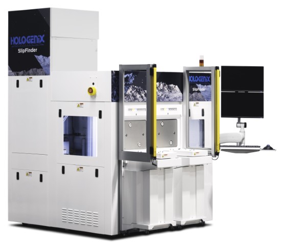
Crystal Slip Defect Detection (SlipFinder)
Hologenix
Fully Automatic 300 mm Wafer Inspection
Defect Detection High Speed Optical Metrology
The SlipFinder is capable of detecting crystal dislocations that occur during many types of wafer processes:
•Epitaxy
•Oxidation, Diffusion
•Post Implant Annealing
•SOI
•Polishing
•Strained Silicon
•Many other Semiconductor Applications
Fully Automatic 300 mm Wafer Inspection
Defect Detection High Speed Optical Metrology
- Fully Automated Defect Detection
- Full or Partial Wafer Inspection
- Adjustable Inspection Recipes
- Sub-micron Detection Sensitivity
- Macro optical Field of View: 15mm X 12mm
- Throughput: Approx 15 – 80 WPH
- Dual FOUPs; Optional FOSB, Open Cassette
- Optical Non-Contact Notch Finding
- Optional class M1 Mini-Environment
- Windows Software Environment
- SECS-GEM via RS232 or HSMS
- Full Factory Automation
- Sorter Capabilities – Optional OCR
- Non-contact Notch, Flat-Finding and Centering Technology
- Software: SlipFinder Advanced Metrology Suite under Windows
- Platform:
o YIS Series: Hologenix YIS300/200
o SF Series: R-Theta-Z Stage - Magic Mirror™ Optics (YIS series & SF300M):
o Macro Field of View: 15mm X 12mm
o Slip Detection Sensitivity: 1-2 mm length - Nomarski (DIC) Optics (SF300N only):
o Micro Field of View (< 3 mm)
o Standard microscope options
Fully Automatic 300 mm Wafer Inspection
Defect Detection High Speed Optical Metrology
- Automated detection of Slip Lines & other defects
- Detect, Count, Locate and Measure (Length)
- Windows Interface
- Adjustable Detection Sensitivity
- Adjustable Edge Exclusion
- Graphic display of wafer with highlighted Slip Sites
- Wafer Accept/Reject recipes
- Lot file Reports, Image Archiving and Printing
- Automated, Semi-Automated and Engineering Mode
- Inspection locations are completely configurable via a Layout/Grid tool.
- All Slip Lines are reported in mm using Wafer Coordinates
- System outputs Wafer Maps showing actual orientation and length of Slip Lines
- Stitching - Sections of Slip Lines from different fields of view can be automatically combined and reported
- System can be configured to stop the Inspection upon failure to improve throughput
- SOI Edge Exclusion measurement capability
The SlipFinder is available in manual, semi-automated, or fully automated system configurations for 100 - 150mm, 150 - 200mm, or 300mm substrate sizes.
Common applications include:
• Epitaxial process control
• Rapid Thermal Processing (RTP, RTA)
• SOI wafer manufacturing
• High temperature diffusion processing